Talk:Kikuchi lines (physics)
A fact from Kikuchi lines (physics) appeared on Wikipedia's Main Page in the Did you know column on 28 April 2008, and was viewed approximately 1,534 times (disclaimer) (check views). The text of the entry was as follows:
|
| This article is rated B-class on Wikipedia's content assessment scale. It is of interest to the following WikiProjects: | |||||||||||
‹See TfM›
| |||||||||||
Items to discuss
[edit]Possible stereographic projection images
[edit]
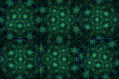
Above find a labeled portion of the Kikuchi map for diamond FFC crystals like Si and Ge, in stereographic projection down the [001] direction. This one was drawn by hand using a beam compass (which even at the time was an arcane piece of equipment) for the large-radius arcs, although it's much easier today to let computers draw the map in 2 or 3 dimensions. Thermochap (talk) 13:25, 25 April 2008 (UTC)

This animation of a stereographic projection follows {220} Kikuchi and/or fringe visibility bands centered on great circles. The centered viewing direction follows those {220} bands between <111> zones, where rotation by 60 degrees sets up travel to the next <111> zone via a repeat of the original sequence. Note how interband angles are locally preserved in the process, even though distances between points vary. Thermochap (talk) 13:25, 25 April 2008 (UTC)
Experimental diffraction images
[edit]
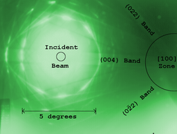
Here's an image of Kikuchi lines leading to a Silicon [100] zone from a beam direction approximately 7.9 degrees away along the (004) Kikuchi band.
Experimental direct-space data
[edit]
Here's a bend contour image, but probably not great for this page -- perhaps better for a page on convergent beam diffraction symmetries than for a page on bend contour and Kikuchi symmetries. Eventually, I imagine that separate pages on bend contours and fringe visibility maps will be warranted as well. Thermochap (talk) 21:13, 28 April 2008 (UTC)

Here's a bend contour down Silicon <111> which shows a larger angular range of bending in the foil. Thermochap (talk) 22:13, 28 April 2008 (UTC)

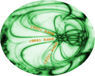
The above (100) spider, trapped in a region of silicon that was shaped like an oval watchglass, was imaged with 300 keV electrons. If you tilt the crystal, the spider moves toward the edges of the oval as though it is trying to get out. The spider's legs, and their intersections can be indexed just like a Kikuchi map.
Footnotes
[edit]What are Kikuchi lines, then?
[edit]The intro needs to be rewritten to properly introduce the term. Starting ‘Kikuchi lines pair up to form bands...’ is quite confusing for a reader who does not already know what Kikuchi lines are. 14:00, 27 September 2017 (UTC)


