Maxwell (microarchitecture)
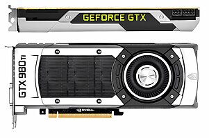
 NVIDIA GeForce GTX 980ti of the GeForce 900-line of graphics-cards, was the final major iteration featuring the Maxwell microarchitecture (GM200-310). | |
| Release date | February 2014 |
|---|---|
| Fabrication process | TSMC 28 nm, 20 nm, 16 nm |
| History | |
| Predecessor | Kepler |
| Successor | Pascal |
| Support status | |
| Supported | |

Maxwell is the codename for a GPU microarchitecture developed by Nvidia as the successor to the Kepler microarchitecture. The Maxwell architecture was introduced in later models of the GeForce 700 series and is also used in the GeForce 800M series, GeForce 900 series, and Quadro Mxxx series, as well as some Jetson products.
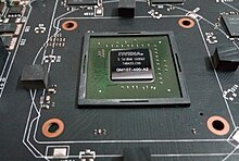
The first Maxwell-based products were the GeForce GTX 745 (OEM), GeForce GTX 750, and the GeForce GTX 750 Ti. Both were released on February 18, 2014, both with the chip code number GM107. Earlier GeForce 700 series GPUs had used Kepler chips with the code numbers GK1xx. First-generation Maxwell GPUs (code numbers GM10x) are also used in the GeForce 800M series and the Quadro Kxxx series. A second generation of Maxwell-based products was introduced on September 18, 2014 with the GeForce GTX 970 and GeForce GTX 980, followed by the GeForce GTX 960 on January 22, 2015, the GeForce GTX Titan X on March 17, 2015, and the GeForce GTX 980 Ti on June 1, 2015. The final and lowest spec Maxwell 2.0 card was the GTX950 released on Aug 20th, 2015. These GPUs have GM20x chip code numbers.
Maxwell introduced an improved Streaming Multiprocessor (SM) design that increased power efficiency,[1] the sixth and seventh generation PureVideo HD, and CUDA Compute Capability 5.2.
The architecture is named after James Clerk Maxwell, the founder of the theory of electromagnetic radiation.
The Maxwell architecture is used in the system on a chip (SOC), mobile application processor, Tegra X1.
First generation Maxwell (GM10x)
[edit]
First generation Maxwell GPUs (GM107/GM108) were released as GeForce GTX 745, GTX 750/750 Ti, GTX 850M/860M (GM107) and GeForce 830M/840M (GM108). These new chips introduced few consumer-facing additional features, as Nvidia instead focused more on increasing GPU power efficiency. The L2 cache was increased from 256 KiB on Kepler to 2 MiB on Maxwell, reducing the need for more memory bandwidth. Accordingly, the memory bus was reduced from 192 bit on Kepler (GK106) to 128 bit, reducing die area, cost, and power draw.[2]
The "SMX" streaming multiprocessor design from Kepler was also retooled and partitioned, being renamed "SMM" for Maxwell. The structure of the warp scheduler was inherited from Kepler, with the texture units and FP64 CUDA cores still shared, but the layout of most execution units were partitioned so that each warp schedulers in an SMM controls one set of 32 FP32 CUDA cores, one set of 8 load/store units and one set of 8 special function units. This is in contrast to Kepler, where each SMX had 4 schedulers that scheduled to a shared pool of execution units.[3] The latter necessitated an SMX-wide crossbar that used unnecessary power to allow all execution units to be shared.[3] Conversely, Maxwell's more modular design allows for a finer-grained and more efficient allocation of resources, saving power when the workload isn't optimal for shared resources. Nvidia claims a 128 CUDA core SMM has 90% of the performance of a 192 CUDA core SMX while efficiency increases by a factor of 2.[2] Also, each Graphics Processing Cluster, or GPC, contains up to 4 SMX units in Kepler, and up to 5 SMM units in first generation Maxwell.[2]
GM107 also supports CUDA Compute Capability 5.0 compared to 3.5 on GK110/GK208 GPUs and 3.0 on GK10x GPUs. Dynamic Parallelism and HyperQ, two features in GK110/GK208 GPUs, are also supported across the entire Maxwell product line. Maxwell also provides native shared memory atomic operations for 32-bit integers and native shared memory 32-bit and 64-bit compare-and-swap (CAS), which can be used to implement other atomic functions.
Nvidia's video encoder, NVENC, was upgraded to be 1.5 to 2 times faster than on Kepler-based GPUs, meaning it can encode video at six to eight times playback speed.[2] Nvidia also claims an eight to ten times performance increase in PureVideo Feature Set E video decoding due to the video decoder cache, paired with increases in memory efficiency. However, H.265 is not supported for full hardware decoding in first generation Maxwell GPUs, relying on a mix of hardware decoding and software decoding (CPU decoding).[2] When decoding video, a new low power state "GC5" is used on Maxwell GPUs to conserve power.[2]
Maxwell GPUs were thought to use tile-based rendering,[4] but they actually use tiled caching.[5]
Since first generation Maxwell, UEFI Graphics Output Protocol is fully supported on NVIDIA GPUs.
Chips
[edit]- GM107
- GM108
Second generation Maxwell (GM20x)
[edit]
Second generation Maxwell GPUs introduced several new technologies: Dynamic Super Resolution,[6] Third Generation Delta Color Compression,[7] Multi-Pixel Programming Sampling,[8] Nvidia VXGI (Real-Time-Voxel-Global Illumination),[9] VR Direct,[9][10][11] Multi-Projection Acceleration,[7] Multi-Frame Sampled Anti-Aliasing(MFAA)[12] (however, support for Coverage-Sampling Anti-Aliasing(CSAA) was removed),[13] and Direct3D12 API at Feature Level 12_1. HDMI 2.0 support was also added.[14][15]
The ROP to memory controller ratio was changed from 8:1 to 16:1.[16] However, some of the ROPs are generally idle in the GTX 970 because there are not enough enabled SMMs to give them work to do, reducing its maximum fill rate.[17]
The Polymorph Engine responsible for tessellation was upgraded to version 3.0 in second generation Maxwell GPUs, resulting in improved tessellation performance per unit/clock.
Second generation Maxwell also has up to 4 SMM units per GPC, compared to 5 SMM units per GPC.[16]
GM204 supports CUDA Compute Capability 5.2 (compared to 5.0 on GM107/GM108 GPUs, 3.5 on GK110/GK208 GPUs and 3.0 on GK10x GPUs).[7][16][18]
GM20x GPUs have an upgraded NVENC which supports HEVC encoding and adds support for H.264 encoding resolutions at 1440p/60FPS & 4K/60FPS (compared to NVENC on Maxwell first generation GM10x GPUs which only supported H.264 1080p/60FPS encoding).[11]
After consumer complaints,[19] Nvidia revealed that it is able to disable individual units, each containing 256KB of L2 cache and 8 ROPs, without disabling whole memory controllers.[20] This comes at the cost of dividing the memory bus into high speed and low speed segments that cannot be accessed at the same time for reads, because the L2/ROP unit managing both of the GDDR5 controllers shares the read return channel and the write data bus between the GDDR5 controllers. This makes simultaneous reading from both GDDR5 controllers or simultaneous writing to both GDDR5 controllers impossible.[20] This is used in the GeForce GTX 970, which therefore can be described as having 3.5 GB in a high-speed segment on a 224-bit bus and 512 MB in a low-speed segment on a 32-bit bus.[20] The peak speed of such a GPU can still be attained, but the peak speed figure is only reachable if one segment is executing a read operation while the other segment is executing a write operation.[20]
Chips
[edit]- GM200
- GM204
- GM206
Performance
[edit]The theoretical single-precision processing power of a Maxwell GPU in FLOPS is computed as 2 (operations per FMA instruction per CUDA core per cycle) × number of CUDA cores × core clock speed (in Hz).
The theoretical double-precision processing power of a Maxwell GPU is 1/32 of the single precision performance (which has been noted as being very low compared to the previous generation Kepler).[21]
Successor
[edit]The successor to Maxwell is codenamed Pascal.[22] The Pascal architecture features higher bandwidth unified memory and NVLink.[22]
See also
[edit]- List of eponyms of Nvidia GPU microarchitectures
- List of Nvidia graphics processing units
- Nvidia NVDEC
- Nvidia NVENC
References
[edit]- ^ "5 Things You Should Know About the New Maxwell GPU Architecture". 2014-02-21.
- ^ a b c d e f Smith, Ryan; T S, Ganesh (18 February 2014). "The NVIDIA GeForce GTX 750 Ti and GTX 750 Review: Maxwell Makes Its Move". AnandTech. Archived from the original on 18 February 2014. Retrieved 18 February 2014.
- ^ a b Ryan Smith, Ganesh T S. "Maxwell: Designed For Energy Efficiency - The NVIDIA GeForce GTX 750 Ti and GTX 750 Review: Maxwell Makes Its Move".
- ^ Kanter, David (August 1, 2016). "Tile-based Rasterization in Nvidia GPUs". Real World Technologies. Retrieved April 1, 2016.
- ^ "On NVIDIA's Tile-Based Rendering". Tech Power Up. March 1, 2017. Retrieved May 9, 2020.
- ^ "Dynamic Super Resolution Improves Your Games With 4K-Quality Graphics On HD Monitors". www.nvidia.com.
- ^ a b c "Archived copy" (PDF). Archived from the original (PDF) on 2017-07-21. Retrieved 2014-09-19.
{{cite web}}: CS1 maint: archived copy as title (link) - ^ "NVIDIA BatteryBoost: Ditch the Brick". NVIDIA.
- ^ a b "GeForce Articles, Guides, Gaming News, Featured Stories". www.nvidia.com.
- ^ "How Maxwell's VR Direct Brings Virtual Reality Gaming Closer to Reality". The Official NVIDIA Blog.
- ^ a b Ryan Smith. "Display Matters: HDMI 2.0, HEVC, & VR Direct - The NVIDIA GeForce GTX 980 Review: Maxwell Mark 2".
- ^ "Multi-Frame Sampled Anti-Aliasing Delivers Better Performance To Maxwell Gamers". www.nvidia.com.
- ^ "New nVidia Maxwell chips do not support fast CSAA".
- ^ "GeForce RTX 20 Series Graphics Cards and Laptops". NVIDIA.
- ^ Ryan Smith. "The NVIDIA GeForce GTX 980 Review: Maxwell Mark 2".
- ^ a b c Ryan Smith. "Maxwell 2 Architecture: Introducing GM204 - The NVIDIA GeForce GTX 980 Review: Maxwell Mark 2".
- ^ "Here's another reason the GeForce GTX 970 is slower than the GTX 980". The Tech Report.
- ^ "Maxwell: The Most Advanced CUDA GPU Ever Made". Parallel Forall. 19 September 2014.
- ^ Geoffrey Tim (3 December 2015). "Nvidia's GTX970 has a rather serious memory allocation bug". Lazygamer.net.
- ^ a b c d Ryan Smith. "Diving Deeper: The Maxwell 2 Memory Crossbar & ROP Partitions - GeForce GTX 970: Correcting The Specs & Exploring Memory Allocation".
- ^ Smith, Ryan (17 March 2015). "The NVIDIA GeForce GTX Titan X Review". AnandTech. p. 2. Retrieved 6 December 2015.
...puny native FP64 rate of just 1/32
- ^ a b "NVIDIA Updates GPU Roadmap; Announces Pascal". The Official NVIDIA Blog.
