TO-92
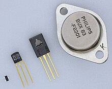
The TO-92 is a widely used style of semiconductor package mainly used for transistors. The case is often made of epoxy or plastic, and offers compact size at a very low cost.
History and origin
[edit]The JEDEC TO-92 descriptor is derived from the original full name for the package: Transistor Outline Package, Case Style 92.[1] The package is also known by the designation SOT54. By 1966 the package was being used by Motorola for their 2N3904 devices among others.[2]
Construction and orientation
[edit]
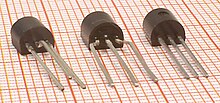
The case is molded around the transistor elements in two parts; the face is flat, usually bearing a machine-printed part number (some early examples had the part number printed on the top surface instead). The back is semi-circularly-shaped. A line of moulding flash from the injection-moulding process can be seen around the case.
The leads protrude from the bottom of the case. When looking at the face of the transistor, the leads are commonly configured from left-to-right as the emitter, base, and collector for 2N series (JEDEC) transistors, however, other configurations are possible, such as emitter, collector, and base commonly used for 2S series (Japanese) transistors or collector, base, and emitter for many of the BC series (Pro Electron) types.
If the face has a part name made up of only one letter and a few numbers, it can be either a Japanese or a Pro Electron part number. Thus, "C1234" would likely be a 2SC1234 device, but "C547" is usually short for "BC547".

The leads coming out of the case are spaced 0.05" (1.27 mm) apart. It is often convenient to bend them outward to a 0.10" (2.54 mm) spacing to make more room for wiring.[3] Units with their leads pre-bent may be ordered to fit specific board layouts, depending on the application. Otherwise, the leads may be bent manually; however, care must be taken as they can break easily, as with any other device that is manually configured.
The physical dimensions of the TO-92 housing may vary slightly depending on the manufacturer, however, the 1.27mm lead spacing must be respected.
Advantages
[edit]- Transistors of this type can be made very inexpensively and take up very little board space. Most models are readily available in large quantities from wholesale distributors.
- They are easy to find in small electronics stores because of their wide usefulness, making them a popular choice for hobby work and prototyping.
Disadvantages
[edit]The main disadvantage of this style of case is the lack of heat sinking.
- Transistors and ICs of these types cannot handle as much power as higher-power equivalents, such as the TO-220, and can burn out quickly if they dissipate excessive power.
- There is no standard pinout for the TO-92. The American BJTs use the E-B-C pinout while their Japanese counterparts use the E-C-B pinout and some RF devices use the B-E-C pinout.[citation needed]
Voltage and current
[edit]Although TO-92 devices are mainly used in low-voltage / low-current (<30 V; <1 A) applications, high-voltage (600 Volt Vce) and high-current (5 A Ic) devices are available. Nominal maximum power dissipation is less than one watt (600 mW).
Variants
[edit]For diodes or integrated circuits with two connections (e.g. temperature sensors) the middle lead is either not connected or omitted entirely.

In the late 1960s, Ferranti introduced a smaller package with a compatible footprint, called "E-Line".[4][5] This package was later standardized as a British Standard (but not by JEDEC) and remained in production with Ferranti Semiconductors' successor companies (Plessey, Zetex Semiconductors, Diodes Incorporated[6]). In East Germany the E-Line package was known as the "Miniplast" package and widely used by Kombinat Mikroelektronik Erfurt.
Standards
[edit]| Standards organization | Standard | Designation for | ||
|---|---|---|---|---|
| TO-92 | E-Line/Miniplast | |||
| 3-lead | 2-lead | |||
| IEC | IEC 60191[7] | A68 | ||
| DIN | DIN 41868[8] | 10B3[a] | ||
| EIAJ / JEITA | ED-7500A[9][10] | SC-43A | ||
| British Standards | BS 3934[11] | SO-94[b] | ||
| Gosstandart | GOST 18472—88[12] | KT-26[c] | — | KD-129[d] |
| Rosstandart | GOST R 57439—2017[13] | |||
| Kombinat Mikroelektronik Erfurt | TGL 200-8380[14] | — | — | L2 |
| TGL 11811[7] | — | L3 | — | |
| TGL 26713/07[7] | F2 | F3 | F4 | |
- ^ DIN 41868 also defines variants with the leads bent to emulate the footprint of other packages: 10A3 (TO-18 footprint).
- ^ BS-3934 also defines variants with the leads bent to emulate the footprint of other packages: SO-95 (TO-5 footprint), SO-96 (for flat mounting), and SO-97 (TO-18 footprint).
- ^ Russian: КТ-26
- ^ Russian: КД-129
Common components in a TO-92 package
[edit]Common transistors:
- BC548, general purpose NPN transistor
- BC558, general purpose PNP transistor
- 2N3904, general purpose NPN transistor
- 2N3906, general purpose PNP transistor
- 2N7000, N-channel FET
- BS170, N-channel FET, similar to 2N7000
- PN2222A, a "plastic" version of the original 2N2222 NPN transistor which came in a TO-18 package
Other common components:
- MK484, AM radio integrated circuit
- 78Lxx series, voltage regulator integrated circuits
- TL431, voltage regulator integrated circuit
References
[edit]- ^ a b c "JEDEC TO-92 package specification" (PDF). JEDEC. Archived from the original (PDF) on June 18, 2017.
- ^ The semiconductor data book. Motorola. August 1966. Retrieved 2021-07-09.
- ^ Bourns. "Package Mechanical Information, TO-92" (PDF). Retrieved 28 February 2016.
- ^ Applications of the E-Line Plastic Encapsulated Transistor. Oldham: Ferranti Ltd. June 1969. Retrieved 2021-07-10.
- ^ "E-Line – The ultimate TO-92". Quick Reference Guide (PDF). Ferranti Semiconductors. February 1983. p. E2. Retrieved 2021-07-10.
- ^ "E-Line Package Information" (PDF). Diodes Incorporated. March 2017. Retrieved 2021-07-10.
- ^ a b c "TGL 26713/07: Gehäuse für Halbleiterbauelemente - Bauform F" [Outline drawings for semiconductor devices; Type F] (PDF) (in German). Leipzig: Verlag für Standardisierung. June 1988. Retrieved 2021-06-15.
- ^ "Semiconductor Databook" (PDF). Heilbronn: AEG-Telefunken. pp. 17, 19. Retrieved 2021-08-20.
- ^ "EIAJ ED-7500A Standards for the Dimensions of Semiconductor Devices" (PDF). JEITA. 1996. p. 120. Retrieved 2021-06-14.
- ^ "TO-92 (SOT54)". Nexperia. 2004-11-16. Archived from the original on 2017-12-13. Retrieved 2021-07-12.
- ^ "Package Outlines". Quick Reference Guide (PDF). Ferranti Semiconductors. February 1983. p. PO14. Retrieved 2021-07-10.
- ^ "ГОСТ 18472—88 ПРИБОРЫ ПОЛУПРОВОДНИКОВЫЕ - Основные размеры" [GOST 18472—88 Semiconductor devices - basic dimensions] (PDF) (in Russian). Rosstandart. 1988. p. 33-34,55. Retrieved 2021-06-17.
- ^ "ГОСТ Р 57439—2017 ПРИБОРЫ ПОЛУПРОВОДНИКОВЫЕ - Основные размеры" [GOST R 57439—2017 Semiconductor devices - basic dimensions] (PDF) (in Russian). Gosstandart. 2017. p. 41-42,68-69. Retrieved 2021-06-17.
- ^ "TGL 200-8380: Halbleiterbauelemente - Halbleiterdioden Verlustleistung unter 1 Watt - Bauformen" [Semiconductor Devices - Designs for Semiconductor Diodes - Dissipation power less 1 Watt] (PDF) (in German). Leipzig: Verlag für Standardisierung. 1981. Retrieved 2021-07-12.
External links
[edit]- TO-92 Package, EESemi.com
- [1] Essay about TO92 housings (German) by Dipl.-Ing. Bernd Wiebus at German national library server.


